- 您现在的位置:买卖IC网 > Sheet目录480 > MTD20P06HDLT4 (ON Semiconductor)MOSFET P-CH 60V 15A DPAK
�� �
�
�MTD20P06HDL�
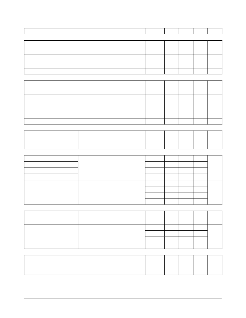
�ELECTRICAL� CHARACTERISTICS� (T� J� =� 25� °� C� unless� otherwise� noted)�
�Characteristic�
�Symbol�
�Min�
�Typ�
�Max�
�Unit�
�OFF� CHARACTERISTICS�
�Drain?Source� Breakdown� Voltage�
�(V� GS� =� 0� Vdc,� I� D� =� 250� m� Adc)�
�Temperature� Coefficient� (Positive)�
�V� (BR)DSS�
�60�
�?�
�?�
�81.3�
�?�
�?�
�Vdc�
�mV/� °� C�
�Zero� Gate� Voltage� Drain� Current�
�I� DSS�
�m� Adc�
�(V� DS� =� 60� Vdc,� V� GS� =� 0� Vdc)�
�(V� DS� =� 60� Vdc,� V� GS� =� 0� Vdc,� T� J� =� 125� °� C)�
�?�
�?�
�?�
�?�
�1.0�
�10�
�Gate?Body� Leakage� Current� (V� GS� =� ±� 15� Vdc,� V� DS� =� 0)�
�I� GSS�
�?�
�?�
�100�
�nAdc�
�ON� CHARACTERISTICS� (Note� 3)�
�Gate� Threshold� Voltage�
�(V� DS� =� V� GS� ,� I� D� =� 250� m� Adc)�
�Temperature� Coefficient� (Negative)�
�Static� Drain?Source� On?Resistance�
�V� GS(th)�
�R� DS(on)�
�1.0�
�?�
�?�
�1.7�
�3.9�
�143�
�2.0�
�?�
�175�
�Vdc�
�mV/� °� C�
�m� W�
�(V� GS� =� 5.0� Vdc,� I� D� =� 7.5� Adc)�
�Drain?Source� On?Voltage� (V� GS� =� 5.0� Vdc)�
�V� DS(on)�
�Vdc�
�(I� D� =� 15� Adc)�
�(I� D� =� 7.5� Adc,� T� J� =� 125� °� C)�
�?�
�?�
�2.3�
�1.6�
�3.0�
�2.0�
�Forward� Transconductance� (V� DS� =� 10� Vdc,� I� D� =� 7.5� Adc)�
�g� FS�
�9.0�
�11�
�?�
�mhos�
�DYNAMIC� CHARACTERISTICS�
�Input� Capacitance�
�C� iss�
�?�
�850�
�1190�
�pF�
�Output� Capacitance�
�Reverse� Transfer� Capacitance�
�(V� DS� =� 25� Vdc,� V� GS� =� 0� Vdc,� f� =� 1.0� MHz)�
�C� oss�
�C� rss�
�?�
�?�
�210�
�66�
�290�
�130�
�SWITCHING� CHARACTERISTICS� (Note� 4)�
�Turn?On� Delay� Time�
�t� d(on)�
�?�
�19�
�38�
�ns�
�Rise� Time�
�Turn?Off� Delay� Time�
�Fall� Time�
�(V� DS� =� 30� Vdc,� I� D� =� 15� Adc,�
�V� GS� =� 5.0� Vdc,R� G� =� 9.1� W� )�
�t� r�
�t� d(off)�
�t� f�
�?�
�?�
�?�
�175�
�41�
�68�
�350�
�82�
�136�
�Gate� Charge�
�(V� DS� =� 48� Vdc,� I� D� =� 15� Adc,�
�V� GS� =� 5.0� Vdc)�
�Q� T�
�Q� 1�
�Q� 2�
�Q� 3�
�?�
�?�
�?�
�?�
�20.6�
�3.7�
�7.6�
�8.4�
�29�
�?�
�?�
�?�
�nC�
�SOURCE?DRAIN� DIODE� CHARACTERISTICS�
�Forward� On?Voltage�
�Reverse� Recovery� Time�
�Reverse� Recovery� Stored� Charge�
�(I� S� =� 15� Adc,� V� GS� =� 0� Vdc)�
�(I� S� =� 15� Adc,� V� GS� =� 0� Vdc,� T� J� =� 125� °� C)�
�(I� S� =� 15� Adc,� V� GS� =� 0� Vdc,�
�dI� S� /dt� =� 100� A/� m� s)�
�V� SD�
�t� rr�
�t� a�
�t� b�
�Q� RR�
�?�
�?�
�?�
�?�
�?�
�?�
�2.5�
�1.9�
�64�
�50�
�14�
�0.177�
�3.0�
�?�
�?�
�?�
�?�
�?�
�Vdc�
�ns�
�m� C�
�INTERNAL� PACKAGE� INDUCTANCE�
�Internal� Drain� Inductance�
�(Measured� from� the� drain� lead� 0.25� ″� from� package� to� center� of� die)�
�Internal� Source� Inductance�
�(Measured� from� the� source� lead� 0.25� ″� from� package� to� source� bond� pad)�
�L� D�
�L� S�
�?�
�?�
�4.5�
�7.5�
�?�
�?�
�nH�
�nH�
�3.� Pulse� Test:� Pulse� Width� ≤� 300� m� s,� Duty� Cycle� ≤� 2%.�
�4.� Switching� characteristics� are� independent� of� operating� junction� temperature.�
�http://onsemi.com�
�2�
�发布紧急采购,3分钟左右您将得到回复。
相关PDF资料
MTD2955VT4
MOSFET P-CH 60V 12A DPAK
MTD3010N
PHOTO DIODE 900NM DOME CLR TO-18
MTD3010PM
PHOTO DIODE 900NM DOME CLR TO-18
MTD3055VL
MOSFET N-CH 60V 12A DPAK
MTD3055V
MOSFET N-CH 60V 12A DPAK
MTD5010N
PHOTO DIODE 850NM DOME CLR TO-18
MTD5010W
PHOTO DIODE 850NM FLAT CLR TO-18
MTD5052N
PHOTO DIODE 525NM B/G CLR TO-18
相关代理商/技术参数
MTD214
制造商:未知厂家 制造商全称:未知厂家 功能描述:Ethernet Encoder/Decoder and 10BaseT Transceiver with Built-in Waveform Shaper
MTD2525J
制造商:SHINDENGEN 制造商全称:Shindengen Electric Mfg.Co.Ltd 功能描述:DMOS Microstepping Dual PWM Motor Driver
MTD2955E
制造商:MOTOROLA 制造商全称:Motorola, Inc 功能描述:TMOS POWER FET 12 AMPERES 60 VOLTS RDS(on) = 0.3 OHM
MTD2955ET4
制造商:Motorola Inc 功能描述:
MTD2955V
功能描述:MOSFET DISC BY MFG 2/02
RoHS:否 制造商:STMicroelectronics 晶体管极性:N-Channel 汲极/源极击穿电压:650 V 闸/源击穿电压:25 V 漏极连续电流:130 A 电阻汲极/源极 RDS(导通):0.014 Ohms 配置:Single 最大工作温度: 安装风格:Through Hole 封装 / 箱体:Max247 封装:Tube
MTD2955V1
制造商:ON Semiconductor 功能描述:Trans MOSFET P-CH 60V 12A 3-Pin(3+Tab) IPAK Rail
MTD2955V-1
制造商:ONSEMI 制造商全称:ON Semiconductor 功能描述:Power MOSFET 12A, 60V P-Channel DPAK
MTD2955V-1G
制造商:ONSEMI 制造商全称:ON Semiconductor 功能描述:Power MOSFET 12A, 60V P-Channel DPAK